Hi again  This may get a little off-topic and even more techie at some parts. This may get a little off-topic and even more techie at some parts.
This is a "spin off" thread from this thread.
The idea is to build an interface for the model1 comm board to do some "blackbox" testing.
For the sake of simplicity, I choose the IBM PC's ISA-bus, as it features a lot of control logic that we need.
The basic idea is to use a (rather) small I/O area to access the model1 comm boards "host" port.
Logic - Ideas
The model1 comm board features an 21 bit address bus (A0 to A20) and 16 bit data bus (D0 to D15), there are several other control signals, as IOW-, IOR-, VINT-, EX1- and EXWAIT-.
And of course there is a 32M pin for the 32MHz OSC on the model1 cpu board.
I came up with a rather simple "glue" logic.
(please note - this image is neither correct nor complete )
Hardware
The model1 comm board features an 21 bit address bus (A0 to A20) and 16 bit data bus (D0 to D15).
These 21 address bits are grouped:
- A0 to A12
- A16 to A20
A1 to A11 are connected to the shared memory chips - nothing special about it.
A1, A12, (A0 or A16), (A17 or A18), A19, A20, EX1-, IOR- and IOW- are connected to IC6 - a PAL18 which serves as address decoder.
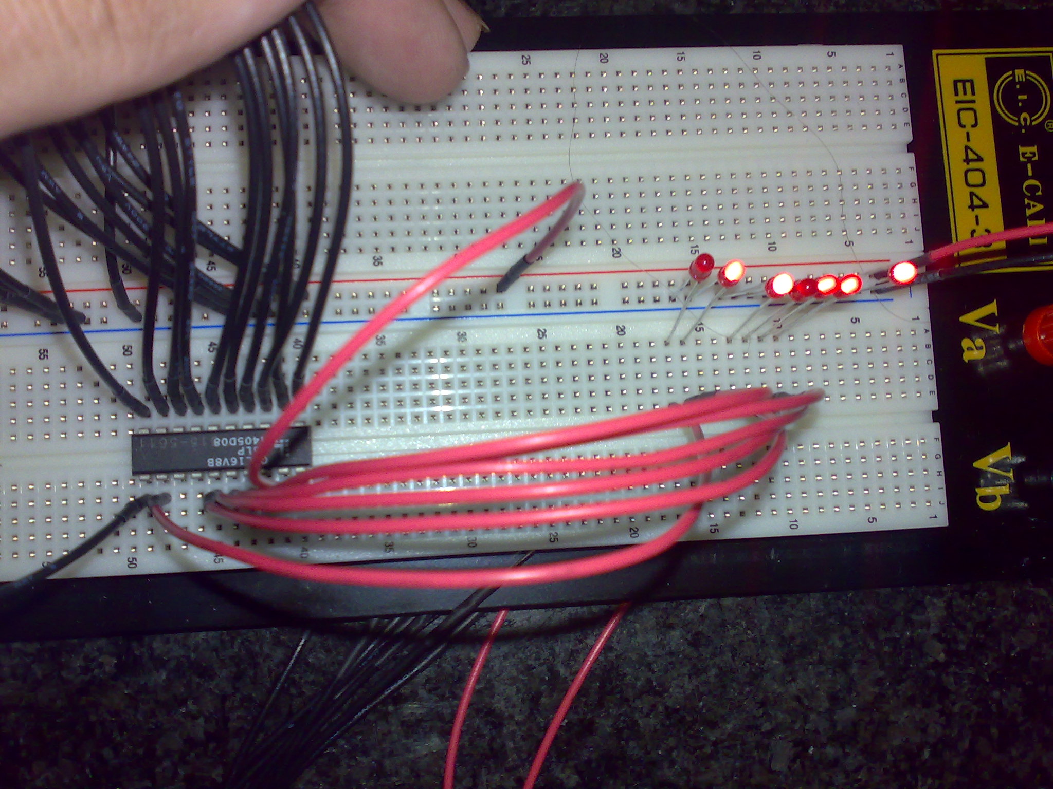
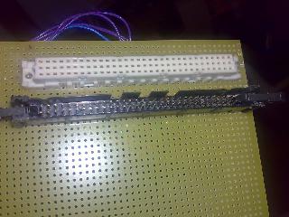
So the idea was to read out the PAL and check what it does... I don't get that JEDEC stuff, so I used a rather "hacky" approach - with breadboard and some wires
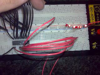
As it turns out - A16 to A19 need to be "low", A20 and EX1 need to be "high" - to select the comm board in any way.
The comm board is "mapped" in the model1 address space at 0xB00000 so we can guess which address bits would be used.
Code:
HEX     BIT
B00000  1011 0000 0000 0000 0000 0000
...
B01000  1011 0000 0001 0000 0000 0000
...

        2222 1111 1111 1100 0000 0000
        3210 9876 5432 1098 7654 3210
           + ----    x xxxx xxxx xxxx
That leads to this:
Code:
Read  @ B00000 = MEMR
Write @ B00000 = MEMW
...
Read  @ B00FFF = MEMR
Write @ B00FFF = MEMW
Read  @ B01000 = CNRD (Bit0)
Write @ B01000 = CNWR (Bit0)
Read  @ B01002 = FGRD (Bit0 & Bit7 [ZFGWR])
Write @ B01002 = FGWR (Bit0)
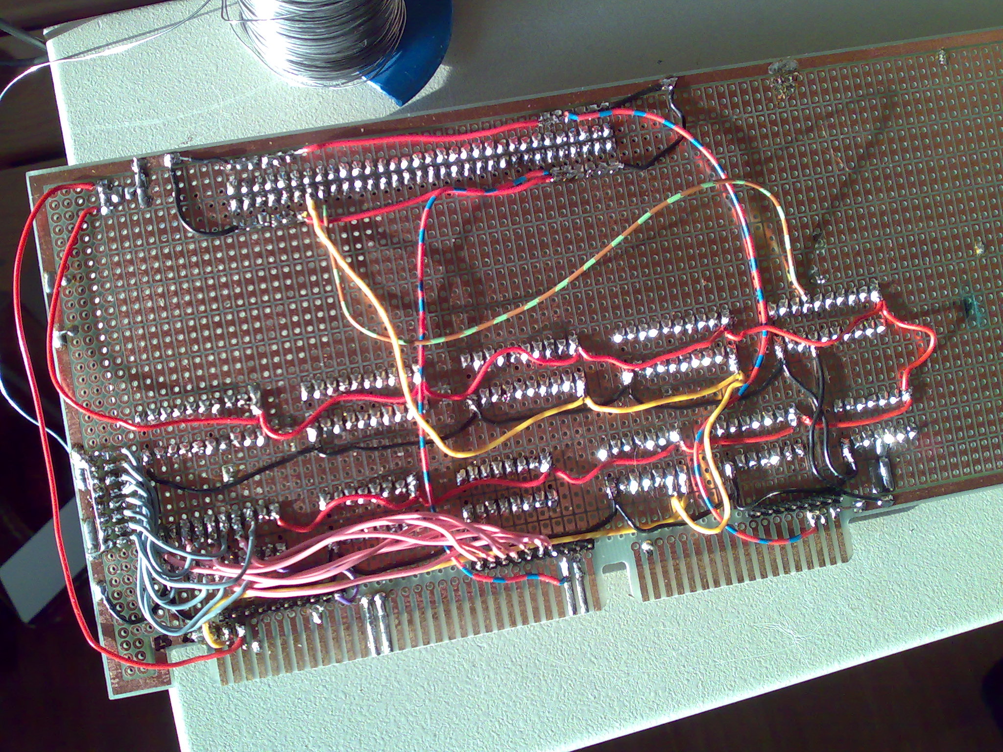
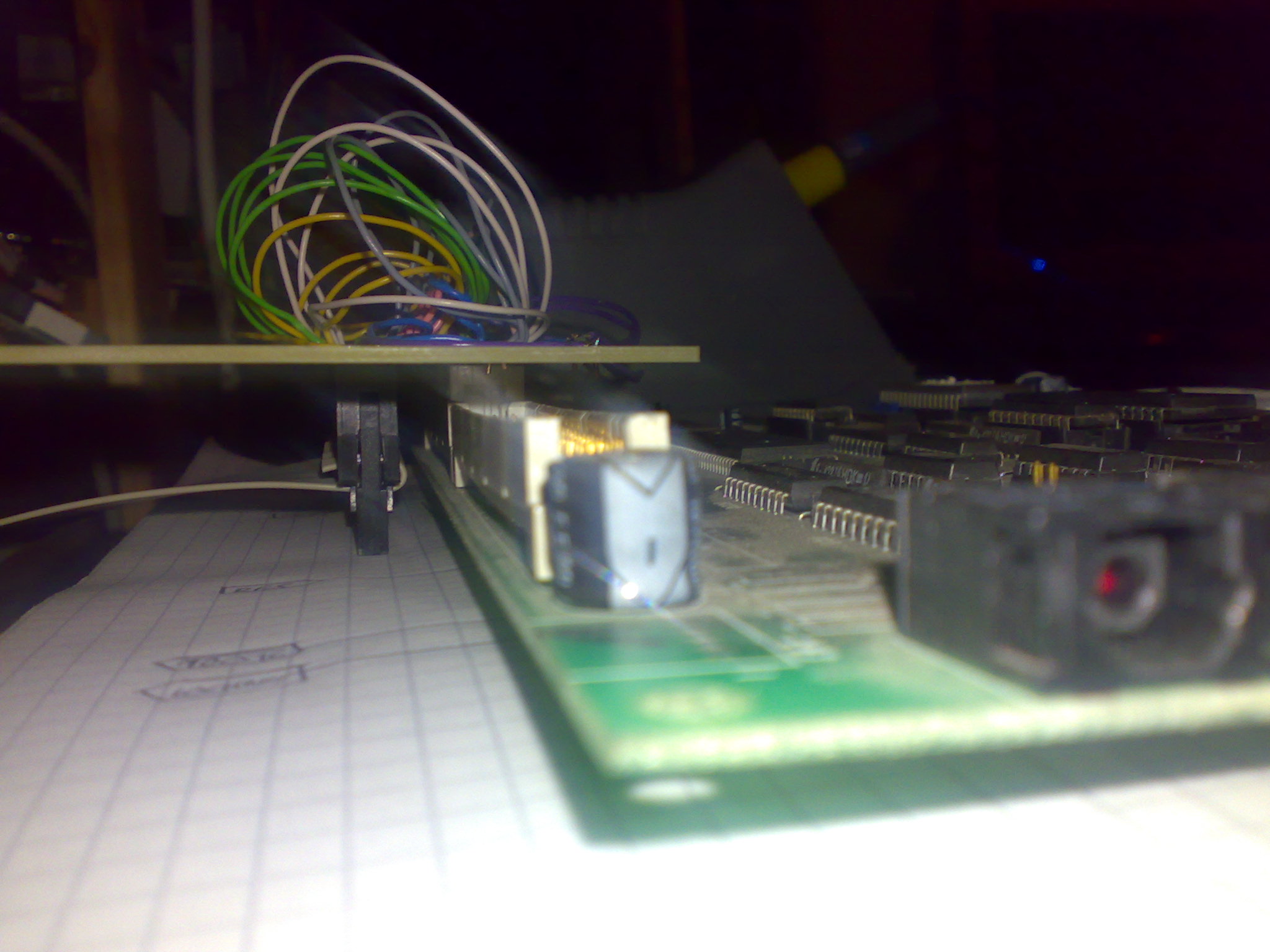
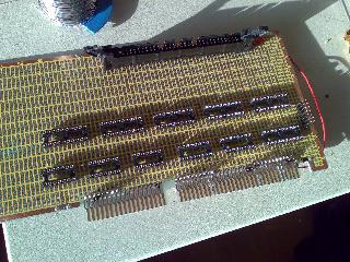
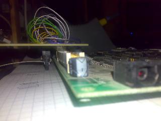
Bridgeboard - ISA side
The bridgeboard is rather simple.
For the 32MHz signal I used a 32MHz OSC... quite simple huh? 
I use a 74682 as "chip select" decoder for the ISA-bus.
P-Signal use A3 to A9 and AEN signals.
Q-Signal uses 7 Jumpers and GND.
If P equals Q we know our bridge is accessed - IOCS- goes "low".
I also use two 74138 as read- and write-address decoder.
ABC-Inputs are connected with A0 to A2.
G2A- is connected to CS-.
G2B- is connected to IOR- / IOW-.
I only use the Y0- and Y2- outputs - W0-/W2- and R0-/R2-.
As this is a 16 bit capable card, I need to pull down IOCS16-.
Also, if the comm boards memory is "busy", I need to pull down IOCHRDY.
For that, I use a 74125 and a 7432.
CS- is used to connect IOCS16- to GND.
(CS- or EXWAIT-) is used to connect IOCHRDY to GND.
This works because both signals CS- and EXWAIT- need are "active low", and the OR-gate output gets "low" only if both inputs are "low" too.
As for some other control signals.
The ISA-bus has a RESET signal, and the model1 comm board uses a RES- signal.
I simply invert the signal using an 7404.
To latch the address, I use two 74273.
W2- signal is used to "update" the latched address.
the outputs are connected to the comm boards address lines A0 to A15
As I don't have any VSYNC signal on the ISA bus I choose to use R2- as VINT- signal. More on this one later.
W0- is connected to the comm boards IOW- line.
R0- is connected to the comm boards IOR- line.
I planed to generate a valid EX1- signal like this:
W0- and R0- get inverted by the 7404, both signals are then fed to the 7432 - the ORed result is then inverted again (7404) and thus used as EX1-.
However, in the end I became lazy and simply connected EX1- to GND
The data lines are connected to both the 74273 inputs as well as the comm boards data lines D0 to D15.
At first I used two 74645 bus gates - however I removed them later as they are not needed.
  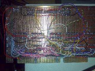  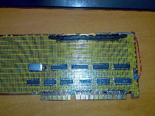
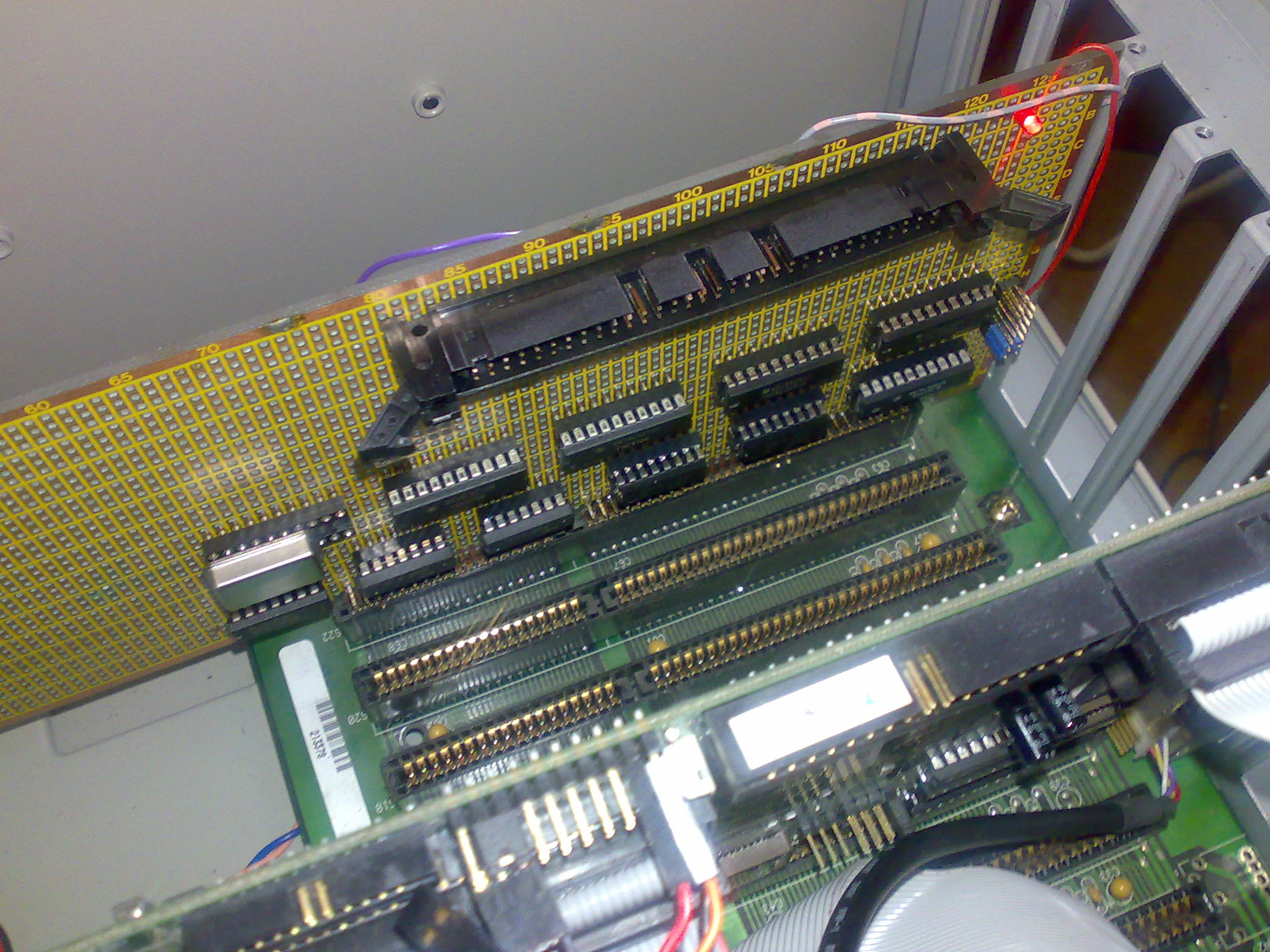
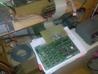
At last... nothing blew up after plugin it in for the first time 
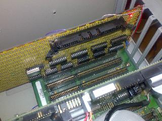
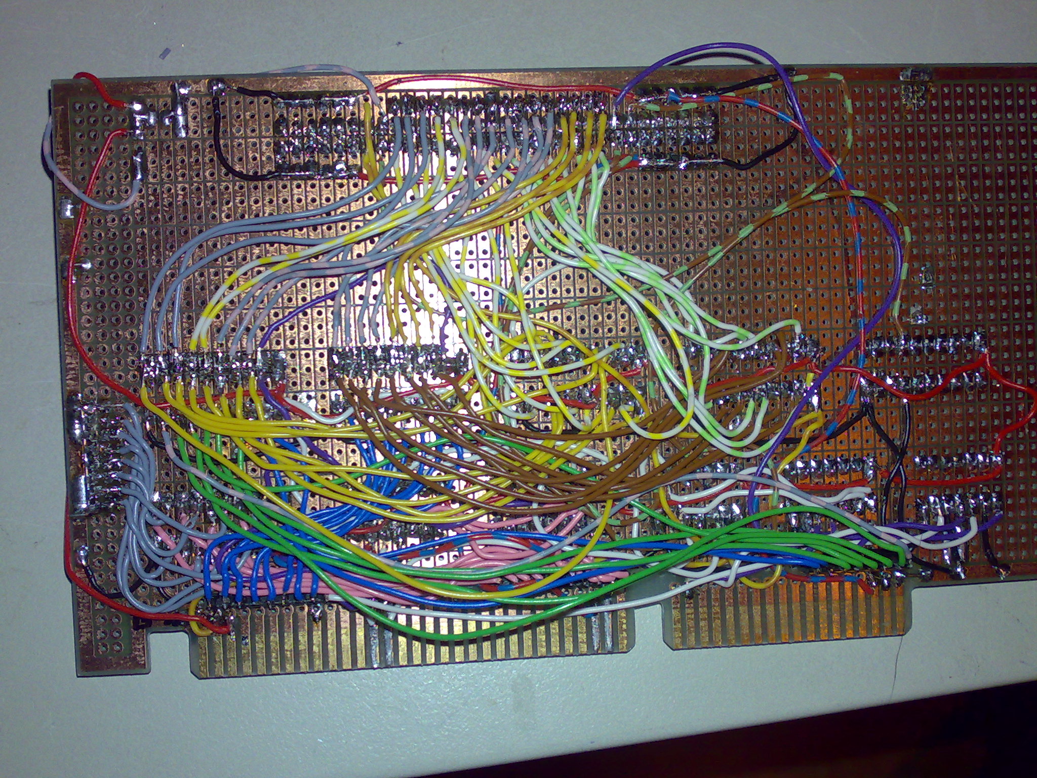
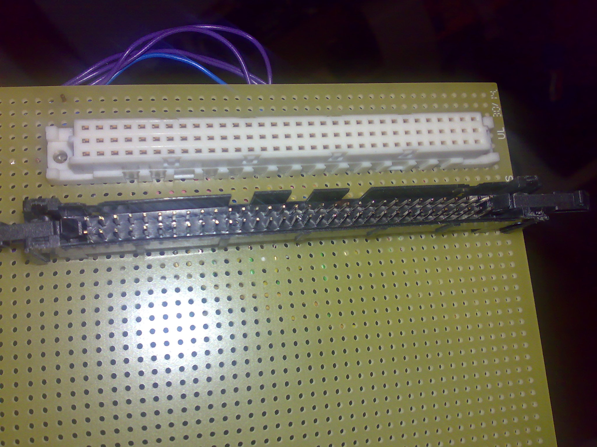
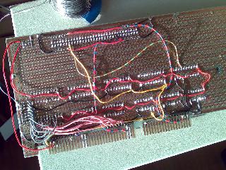
Bridgeboard - model1 comm board side
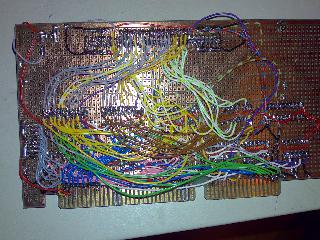
The "other" side of the bridge is a simple (still messy) wire adapter.
It simply plugs into the comm board
(Phew... nothing blew up )
Software side
As for the PC side, the bridgeboard is located at IO 0x300 to 0x307:
Writes to 0x302 update the address latches (16 bit).
Reads from 0x302 trigger a VINT-. (theoretical - should be about 58hz?)
Reads/Writes to 0x300 are processed by the comm board.
So if I want to read data located at 0x0123 from the comm boards shared memory...
I write 0x0123 to 0x302 and then read from 0x300.
One thing I didn't actually pay attention to, is the endianess. My Intel CPU (as well as the comm boards Z80) use little-endian. However I don't know what the NEC V60 used on the model1 cpu board does.
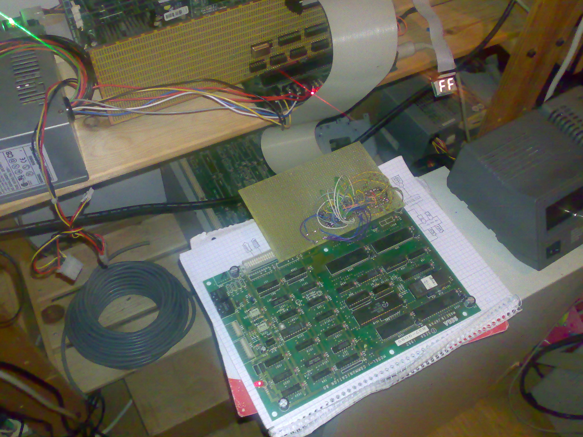
I did some simple tests routines (in Visual Basic ^^) to check the bridgeboard.
I can access both CN (0x1000) and FG (0x1002) "registers" without problems.
My SRAM test (reads and writes from/to 0x0000 to 0x0FFF) indicates that this is working too - however the memory at 0x0000 always returns 0xFF.. which I suppose gets writen there by the comm boards Z80.
No further tests have been done yet.
I do all that stuff even without a Joystick
Soft-15kHz, cabMAME, For Amusement Only e.V.
|

 Flat
Flat  This may get a little off-topic and even more techie at some parts.